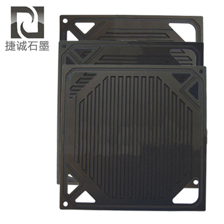
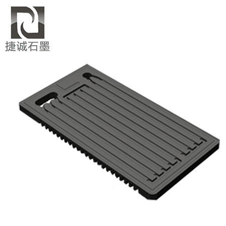
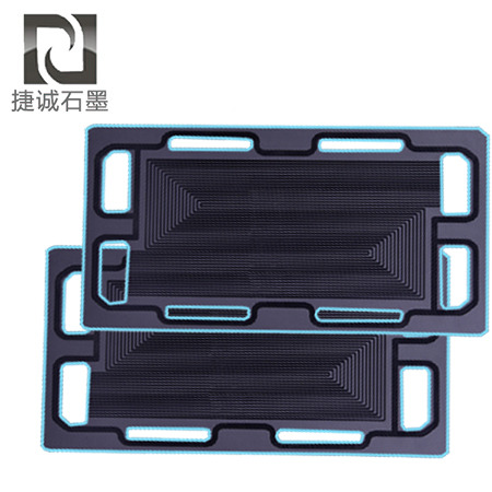
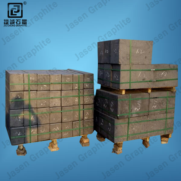
Semiconductor manufacturing imposes far stricter standards on graphite parts compared with general industrial scenarios such as photovoltaic thermal fields and metallurgy. When customizing graphite components, photovoltaic crystal pulling thermal field parts prioritize cost and dimensional control, while semiconductor epitaxy susceptors, SiC crystal growth crucibles and etching electrodes rely heavily on purity, ash content, metallic impurity control and thermal uniformity as core success factors. Many buyers fail to clarify these requirements at the early inquiry stage, resulting in inaccurate quotations, unusable delivered parts and even production line contamination. This article lists technical parameters and cleanliness specifications to confirm for custom semiconductor graphite parts, for item-by-item verification before order placement.
1. Purity and Ash Content: The Primary Threshold
The key distinction between semiconductor-grade graphite and ordinary high-purity graphite lies in tighter control of ash content, metallic impurities and batch consistency. Common reference indicators in industry literature include:
Ash content controlled at ppm level, e.g. ≤5 ppm
Purity of 99.999% (5N) or higher
It should be noted that these figures are general reference ranges. Final specifications must follow your process requirements. Different processes (crystal growth thermal field, epitaxy susceptors, etching electrodes) have varying sensitivity to impurity types. Alkali metals and heavy metals can cause contamination even at extremely low concentrations in certain semiconductor processes.
Verification methods shall be agreed in advance. Graphite purity is characterized by carbon content, while ash content and metallic impurities are commonly tested by third-party elemental analysis such as ICP-OES. Clarify in contracts who conducts testing, which test standard is adopted, and whether certificates are issued per batch or on a sampling cycle.
2. Physical Material Parameters: Confirm Item by Item, Do Not Rely Only on Grade Names
Typical parameters of commercially available custom semiconductor graphite parts serve as a starting point for communication. Values vary widely across manufacturers and grades, so verify each indicator separately:
| Parameter | Typical Reference Value |
|---|---|
| Bulk density of isostatic graphite | Approx. 1.75 g/cm³ |
| Flexural strength | ≥45 MPa |
| Thermal conductivity (high-purity plate) | 100–150 W/m·K (grade-dependent) |
| CNC machining tolerance | Approx. ±0.02 mm |
| Surface roughness (fine polishing) | Down to Ra0.4 |
3. Machining and Inspection Capability: The Dividing Line for Complex Shaped Parts
Semiconductor graphite components usually feature sophisticated structures, such as epitaxy susceptors with positioning holes, thin-wall crucibles and electrodes with flow channels. Evaluate manufacturers on these points:
Machining envelope: whether the maximum processing size and minimum feature size cover your part geometry
Stable repeatability of tolerance and surface finish: not all factories can consistently deliver ±0.02 mm precision and Ra0.4 fine polishing in mass production
Inspection equipment: availability of CMM and capability to issue inspection reports for critical dimensions
Post-treatment capacity: whether purification, impregnation, SiC or PyC coating are completed in-house or outsourced, and the quality control protocol for outsourced processes
For cleanliness-critical applications, confirm cleaning and packaging protocols with your supplier before ordering, such as whether clean packaging is adopted and whether deionized water cleaning is performed prior to packing. Practices differ across factories; these terms must be documented before order confirmation rather than raised after delivery.
4. Refined Requirements by Process Application
Even within semiconductor manufacturing, priorities differ for different graphite parts:
Crystal growth thermal field parts (e.g. SiC crystal growth crucibles): focus on purity, ash control and high-temperature structural stability
Epitaxy susceptors: besides purity, strict demands on dimensional accuracy, surface condition and thermal uniformity
Etching electrodes: emphasize grain structure and anti-erosion performance under electric discharge. Confirm exact parameters with your process team.
Document these application-specific requirements so the manufacturer can match the correct graphite grade and post-treatment solution.
5. Beyond Technical Parameters: Supporting Capabilities Affect Final Quality
Apart from material performance, confirm these supporting capabilities before cooperation:
Traceability and completeness of post-treatment such as purification
Lead time from sampling to mass production
Warranty terms: non-conformance handling and dispute resolution for test disagreements
For export orders: verify whether the supplier has graphite export experience and document-handling competence. Graphite falls under dual-use items; confirm export control requirements with the supplier in accordance with the latest regulations.
Many semiconductor enterprises source from graphite machining industrial clusters. For example, graphite CNC factories in Dongguan have mature supporting resources for complex shaped components. Regardless of supplier location, the above parameter and cleanliness verification workflow remains identical.
Conclusion
The complexity of custom semiconductor graphite parts does not come from a single extreme specification, but the holistic control of purity, ash content, dimensions, surface quality, post-treatment and batch consistency. Convert all above items into formal technical specifications before ordering, and confirm test methods and acceptance criteria line by line with your manufacturer. This safeguards quality and provides evidence for dispute resolution. Industry reference values are only for communication; final specifications must align with your actual process requirements.